(Finance) – New materials for cells photovoltaic innovative and high efficiency that allow the size of the plants to be reduced, but also the costs and environmental impact of the technologies, encouraging technological transfer towards industry. This is what it intends to achieve project GOPVcoordinated by ENEA, in which the universities of Naples “Federico II”, Catania, Perugia, Rome Tor Vergata and Pavia, the Italian Institute of Technology (IIT) and the company participate BeDimensional. The project is financed by the Ministry for the Environment and Energy Security, as part of the activities of the Electrical System Research aimed at technical and technological innovation for the total benefit of users.
Specifically, the GOPV project aims to create devices in silicon And perovskite of the “tandem” type, i.e. which include two cells each designated to effectively absorb a spectral region of light, suitable for building high-yield and small-sized photovoltaic modules.
“The project starts from the considerable know-how of the partners gained in the context of various projects and recognized both nationally and internationally”, declares Paola Delli Veneri, head of the Innovative Devices Laboratory at the ENEA Research Center in Portici. “Furthermore, GOPV represents an opportunity to aggregate the relevant national skills in the sector, promote knowledge on the innovative materials available, eco-friendly and made using low-cost and safe processes, in order to obtain high-efficiency devices and create a new industrial supply chain of photovoltaics”, concludes Delli Veneri.
In particular, researchers will investigate new solutions to increase the sustainability and the stability the performance of the cells, but also the safety of the related production processes.
As for perovskite devices, they will be studied formulations chemicals alternatives to the most commonly used hybrid, organic-inorganic ones, which may contain lead, and which will also be produced through thermal evaporation technologies, to evaluate scalable processes even on larger areas. For silicon ones, however, the project will study new materials to be used in heterojunction cells, which are more transparent than the thin silicon films commonly used. New materials will then be investigated, including two-dimensional ones, capable of offering valid alternatives tooxide Of Indian And pond (ITO), widely used in the electronics and energy sectors, to address any critical issues related to the limited availability of indium. Alongside research on materials and devices, new research infrastructures will also be identified for further development of the results.
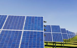
(Photo: Zbynek Burival on Unsplash)